Verilog Sequential RISC-V Processor

Project Overview
This project describes the design and validation of a sequential RISC-V processor – using the Verilog hardware description language (HDL) – capable of executing 20 distinct operations to return 32-bit output values.
Visit my GitHub repository to view all the resources for this project.
Project Objectives
- Design the processor components and containers.
- Encapsulate the components and map all inputs, outputs, and internal buses.
- Validate the processor design.
Engineering Topics
- RISC-V
- Verilog
- Computer Architecture
- Digital Logic
Clicking or tapping a project image opens it at full-size in a new window.
- RISC-V
- Verilog
- Computer Architecture
- Digital Logic
Clicking or tapping a project image opens it at full-size in a new window.
Project Details
Methodology
This processor design incorporates sequential processing of RISC-V instruction types. This lightweight processor performs simple operations, including arithmetic and logical evaluations of two values and the ability to read and write values to/from register and memory locations.
Sequential Processing
This processor adheres to a five-stage pipeline, common to RISC architecture, processing a discrete instruction per cycle. Each instruction passes through all five stages before loading a subsequent instruction – as opposed to pipeline processors, capable of loading subsequent instructions after the previous completes the first stage and mitigating any data hazards caused by multiple instructions performing simultaneous read and write instructions for a register value. This sequential architecture provides the inherited advantage of avoiding such data hazards.
RISC-V Architecture
This processor design adheres to the RISC-V instruction set architecture (ISA) – pronounced “risk five” – with “RISC” denoting its use of “Reduced Instruction Set Computing” and “V” referring to the fifth major iteration of the ISA, developed by UC Berkeley. RISC-V allows for innovation due to its open-source protocol, and it drives speed and efficiency by using smaller instructions that don’t require complex hardware – as opposed to its “Complex Instruction Set Computing (CISC)” counterparts, like x86 and AMD. RISC-V is not a replacement for CISC architecture, but a viable alternative when project requirements warrant a simplicity, flexibility, or energy efficiency. For additional information about RISC-V architecture, visit the RISC-V International website.
RISC-V Instruction Types
RISC-V architecture utilizes a variety of different instructions, categorized by types, that perform specific evaluations and transfer of values between registers (i.e., temporary storage) and memory locations. This processor uses 32-bit instruction values, containing subsets of bits to define the specific instruction actions.
RISC-V architecture allows developers to integrate only the instructions needed for their design – rather than integrating every possible instruction. This processor design contains instructions of the R, I, and S-types – each of which contain subtle formatting differences.
All instruction types begin with an operation code (opcode) that selects the general category for the respective operation. Then, function (funct*) codes – labeled with the number of bits they contain – add specificity to the opcode and designate the target operation.
Each instruction type contains register addresses pointing to read/write values for their operation. The source registers (rs*) refer to the addresses for reading the input values used in the current operation. The destination register (rd) is the address used to write the operation result.
The I and S-type instructions contain immediate (imm) values, referring to a constant value defined within the instruction itself instead of reading a value from a register address.
The instructions for arithmetic operations consider values as signed and logical evaluations as bitwise operations.
R-Type Instructions

R-type (Register) instructions read input values from two registers to perform a single operation (e.g., arithmetic function or logical evaluation) and write the result back to a register. The funct7 value is exclusive to the operation selection for R-type instructions.
The example instruction above represents the addition (ADD) operation, calculating the sum of the values read from source registers 1 and 2, followed by writing the result to register 8.
This processor’s R-type instruction set includes:
- ADD
- AND
- NOR**
- OR
- SEQ**: Set Equal; returns a result when rs1 equals rs2
- SLT: Set Let Than; returns a result when rs1 is less than rs2
- SUB: Subtraction
** The NOR and SEQ instructions are custom expansions of the standard RISC-V ISA.
I-Type Instructions

I-type (Immediate) instructions are like R-type instructions but with a single input from a source register and the other from an immediate value. Not all R-type instructions translate to I-types after substituting the second input value. These I-type exceptions require additional programming to match the behavior of their R-type counterparts. I-type arithmetic and logical operations end with the letter 'I' to differentiate them from their R-type counterparts (e.g., 'ADDI' instead of 'ADD').
The example instruction above is an addition operation, reading one input value from register three, using a constant (immediate) value of '7' for the second input value, and writing their sum to register 7.
The supported I-type instructions for this design include:
- ADDI
- ANDI
- ORI
- SLTI
- LW: Load Word
The I-type instructions include only four operations comparable to the R-type operations and a LW operation that stores data into registers for future calculations, using the destination register address and a relative offset, from its immediate value, to define the data write address. The term “word” in this context refers to a value with a bit width of 32.
S-Type Instructions

The S-type instruction set for this processor includes a Store Word (SW) operation. SW writes data to memory addresses – as opposed to LW, which targets register addresses. Like the I-type instructions, the S-type uses a 12-bit immediate value, but splits and stores this value as two distinct subsets as a workaround to conform with the general RISC-V instruction format.
The SW example above reads the value from rs2 and stores it in memory address 48. The address given in rs1 corresponds to the “zero register (r0),” which contains a constant value of zero in RISC-V architecture. Evaluating the two immediate value subsets together returns a value of 48. So, offsetting the value of 48 from zero returns the memory address value 48 (i.e., 0 + 48 = 48).
Technology
I used Lucidchart to draw schematics for all modules and to map the connections between them. I used Vivado to program all the Verilog modules and validate them using simulation test benches and waveform outputs.
Development
Development of this project began with the design of the Datapath components and the Datapath itself, followed by the Controller modules, and ending with instantiating all design modules and mapping them together within the Processor module. This article presents these steps in reverse, providing high-level aspects of the design that add relevant context to the purpose of lower-level components.

The Processor module is the parent container of this design, containing the two Control modules and the Datapath. This module includes the mapping of signals between its submodules, the system clock and reset input signals, and the result output.
The blue connections represent internal buses between submodules and the connections to/from external input and output signals.
Control Modules

The Controller module interprets the 7-digit Opcode from the current instruction and exports control codes to the ALU Controller and submodules within the Datapath, corresponding to the selection of values or operations within each.
The 2-bit ALU Operation (ALU_Op) signal goes the ALU Controller module, and the following 1-bit signals go to submodules within the Datapath module.
- Register Write (Reg_Write) → Register File (RegFile)
- ALU Source (ALU_Src) → 2:1 Multiplexer, Execution Stage (Mux2_1_EX)
- Memory Read (Mem_Read) and Memory Write (Mem_Write) → Data Memory (DataMem)
- Memory-to-Register (Mem_to_Reg) → 2:1 Multiplexer, Write Back Stage (Mux2_1_WB)

The Arithmetic Logic Unit (ALU) Controller interprets the Function signals (Funct3 and Funct7) from the Datapath and returns the corresponding Operation control code to the ALU within the Datapath. This control code indicates which operation the ALU selects to execute.
Datapath

The Datapath contains a collection of submodules and manages their behavior throughout the five processor stages to execute the current instruction, return the proper result output, and load any subsequent instructions.
Like the Processor module, the Datapath contains port mapping between its subcomponents, the control signals it receives from the Processor and both Control modules, and its output signals for the Control modules and Processor result.
The following subsections describe the modules within each processing stage and their respective behavior.
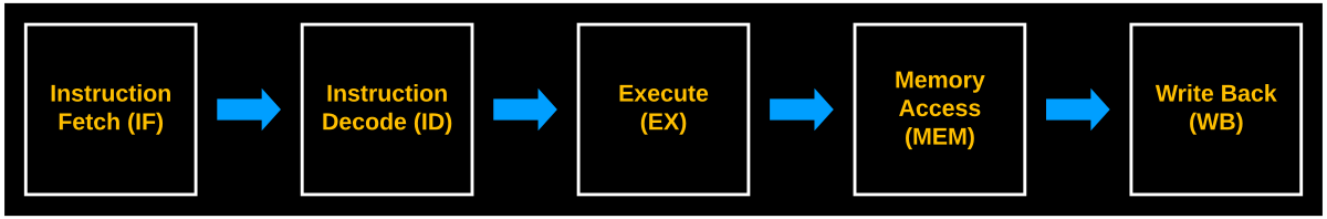
Instruction Fetch (IF) Stage

The Instruction Fetch (IF) stage selects the current instruction from the Instruction Memory module, based on the program counter (PC) signal from the Flip Flop module, in sync with the system clock signal. The Adder sets the address of the next instruction by adding four bits to the current PC and sending this updated value to the Flip Flop.
/** InstrMem.v excerpt: Instruction assignments **/

memory[0]  = 32'b00000000000000000111000000110011; // and  x0,  x0, x0 = 32'h00000000
memory[1]  = 32'b00000000000100000000000010010011; // addi x1,  x0,  1 = 32'h00000001
memory[2]  = 32'b00000000001000000000000100010011; // addi x2,  x0,  2 = 32'h00000002
memory[3]  = 32'b00000000001100001000000110010011; // addi x3,  x1,  3 = 32'h00000004
memory[4]  = 32'b00000000010000001000001000010011; // addi x4,  x1,  4 = 32'h00000005
memory[5]  = 32'b00000000010100010000001010010011; // addi x5,  x2,  5 = 32'h00000007
memory[6]  = 32'b00000000011000010000001100010011; // addi x6,  x2,  6 = 32'h00000008
memory[7]  = 32'b00000000011100011000001110010011; // addi x7,  x3,  7 = 32'h0000000b
memory[8]  = 32'b00000000001000001000010000110011; // add  x8,  x1, x2 = 32'h00000003
memory[9]  = 32'b01000000010001000000010010110011; // sub  x9,  x8, x4 = 32'hfffffffe
memory[10] = 32'b00000000001100010111010100110011; // and  x10, x2, x3 = 32'h00000000
memory[11] = 32'b00000000010000011110010110110011; // or   x11, x3, x4 = 32'h00000005
memory[12] = 32'b00000000010000011010011000110011; // slt  x12, x3, x4 = 32'h00000001
memory[13] = 32'b00000000011100110100011010110011; // nor  x13, x6, x7 = 32'hfffffff4
memory[14] = 32'b01001101001101001111011100010011; // andi x14, x9,  4d3 = 32'h000004d2
memory[15] = 32'b10001101001101011110011110010011; // ori  x15, x11, 8d3 = 32'hfffff8d7
memory[16] = 32'b01001101001001101010100000010011; // slt  x16, x13, 4d2 = 32'h00000001
memory[17] = 32'b01001101001001000100100010010011; // nori x17,  x8, 4d2 = 32'hfffffb2c
memory[18] = 32'b00000010101100000010100000100011; // sw   x11, 48(x0) = 32'h00000030
memory[19] = 32'b00000011000000000010011000000011; // lw   x12, 48(x0) = 32'h00000030, x12 = 32'h00000005
This excerpt from the Instruction Memory (InstrMem.v) module contains the memory assignments for the 20 instruction codes used in the Processor design. The Datapath interprets each instruction, in this order, until completing all of them or being interrupted by the reset signal.
Each instruction includes a comment with its representation in Assembly language and its expected result.
Instruction Decode (ID) Stage

The Instruction Decode (ID) stage receives the instruction values from the previous stage and splits it into several subsets to select the respective register input(s), destination register, and/or immediate value. The Immediate Generator performs a sign extension by repeating the most-significant bit of the input value, the values of which designate whether the value is positive (0) or negative (1).
The output values from this stage include two register values and an immediate value, passed to the next stage, the ALU Controller Function signals and the Controller module Opcode control signal. Like the previous stage, this one also conforms to the system clock and reset signals. The second register value passes to the Memory Access stage as well.
At the end of each cycle, the data from the Write Back phase enters the Register File module and the Register Write Enable signal from the Controller module determines whether to write this value to the specified register address.
Execution (EX) Stage

The Execution (EX) stage passes the first register value to the ALU, along with a second signal of either the other register value or an immediate value, selected by the 2:1 Multiplexer according to the signal received from the Controller module.
The ALU performs one of the following operations, based on the selection value given from the ALU Controller. The ALU result passes through the Datapath and Processor container, and it passes to the Write Back stage. Only the lower nine bits of the result pass to the next phase, which is a unique modification, promoting the simplicity of this design.
Memory Access (MEM) Stage

The Memory Access (MEM) stage reads or writes a memory value, based on the respective control signals received from the Controller module. The ALU result bits from the previous stage designate the read/write address for writing the value received from the ID stage or passing the existing value from this address to the following stage.
Write Back (WB) Stage

The Write Back (WB) stage contains a 2:1 Multiplexer that returns either the memory value read from the previous stage or the ALU result from the Execution phase, depending on the signal received from the Controller module. The selected output returns to the ID Register File for writing to the specified address, if applicable.
Testing
During the module design process, I implemented incremental testing to confirm the functionality of each component through a series of test benches and simulations. For brevity’s sake, this article includes no intermediary testing – only the comprehensive, final design test.
To test the final design, I developed the tb_Processor.v test bench that processes a series of 20 instructions, evaluating the accuracy of each.
The test bench uses three distinct methods to return feedback about the accuracy of results:
- A scoring methodology that assigns one point for each successful result.
- A waveform diagram containing system values over time.
- Console alerts, including output deviations and a final test score.
/** tb_Processor.v scoring and error alerts **/

integer point = 0; // Count for successful cases

/* Test Cases */
always @(*) begin
    #20;
    if (result_tb == 32'h00000000) point = point + 1;
    else $display("FAIL! memory[0] = %h", result_tb);


    /* Evaluations for all remaining results */


end

/* Summary message */
$display ("%s%0d","Number of correct test cases: ", point);
This excerpt of code from the test bench shows the logic for scoring successful results and printing Tcl output for invalid ones and an example of a result evaluation. After a brief delay before each evaluation, the test bench compares the actual and expected results from each test case. It adds one point for each successful test and prints an error message to the Tcl for each incorrect one, which includes the actual result value.
The point value assignments use blocking logic to mitigate the risk of evaluating the incorrect result at the rising clock edge when the result value changes from one instruction to the next.
After evaluation all the test cases, It prints a summary message that includes the number of successful test cases.
## Example Tcl Output

FAIL! memory[0] = 00000001

Number of correct test cases: 19
This hypothetical Tcl output includes an example error message from the first test and a summary message indicating the accuracy of the remaining 19 results. The expected result for the first test is 0x00000000, but the error message returns an actual value of 0x00000001.
Again, this is a hypothetical example, containing an error message. The actual simulation returned no error messages and 20 correct test cases.
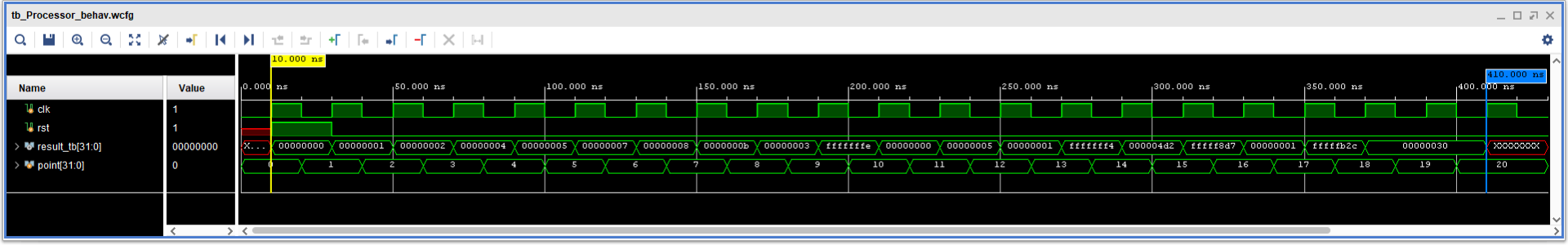
This waveform diagram is an example of the final simulation output, illustrating the correct results from each of the 20 test cases. As previously mentioned, new results correspond with the rising clock edge – after initializing the system with a reset signal.
These three methods work together, giving high-level performance feedback from the summary, identifying specific errors with alerts, and providing context of the entire system via the waveform diagram.
Credits
This project is the optimization of the final project I developed for the “Introduction to Digital Logic Laboratory (EECS 31L)” course I completed at the Samueli School of Engineering at UC Irvine.
References
Project Results
The combined results from the three testing methods, within the final test bench, confirmed the Processor design performed all tasks with 100% accuracy. The scoring method returned all 20 points, the waveform illustrated the expected sequence of operations and results at the appropriate times, and the simulation returned no error messages.
Next Steps
This sequential processor design presents the opportunities to scale its capabilities by increasing the number of R, I, and S-type instructions it supports, and expanding its design to support additional RISC-V instruction types, like J-type – or “jump” – instructions.
In addition to scaling the breadth of instructions, expanding the depth of the instruction memory is a viable option to increase the overall number of instructions executed by the processor.
Conversely, reducing the instruction breadth and optimizing the instruction depth is an effective use case for modifying the design to support a specific hardware solution, while reducing unnecessary overhead resulting from unnecessary features.
The greatest opportunity for this design – or a modified version thereof – is transferring it to a field-programmable gate array (FPGA) for the purpose of driving hardware components and systems.
Feedback
Thank you for reviewing my project. I hope you found it insightful. Please contact me if you have any questions or feedback about this specific project – or my work in general.
Recent Projects
If you enjoyed this project, please consider reviewing one of my recent projects below.
