Verilog Pipelined MIPS32 Processor

Project Overview
This project focuses on the design and validation of a pipelined MIPS32 processor, capable of executing multiple simultaneous instructions with controls to mitigate potential data hazards. This design uses the Verilog hardware description language (HDL) and contains instructions that perform arithmetic and logical evaluations, branch and jump operations, and the loading and storing of values to/from register and memory addresses. The basis of this design is an educational MIPS framework that may vary from more sophisticated implementations in certain areas.
The MIPS32 architecture used for this design is similar to the architecture used in my Verilog Sequential RISC-V Processor design. I recommend reviewing that project prior to reading this article because this one includes references to concepts from the previous project to eliminate the need for redundant descriptions.
Visit my GitHub repository to view all the resources for this project.
Project Objectives
- Design a five-stage MIPS processor.
- Integrate hazard mitigation units.
- Validate the processor performance and hazard responses.
Engineering Topics
- MIPS
- Verilog
- Computer Architecture
- Digital Logic
Clicking or tapping a project image opens it at full-size in a new window.
- MIPS
- Verilog
- Computer Architecture
- Digital Logic
Clicking or tapping a project image opens it at full-size in a new window.
Project Details
Methodology
This processor design uses a simplified implementation of the MIPS32 architecture framework, which is a predecessor to modern instruction set architectures (ISAs), like the RISC-V ISA I used in my previous Verilog processor design. Initially, MIPS was an acronym for “Microprocessor without Interlocked Pipelined Stages,” but now the acronym is synonymous with the company that developed the framework instead of its literal and initial meaning – like using the name “KFC” instead of “Kentucky Fried Chicken.” The “32” in MIPS32 refers to its 32-bit implementation.
Unlike my previous, RISC-V processor design, this MIPS32 processor design uses pipelining to load, execute, and store the results of multiple, simultaneous instructions – as opposed to the complete processing of a single instruction before loading subsequent instructions.
MIPS Instruction Types
The MIPS processor uses 32-bit instructions from three categories: R, I, and J-type. The first two resemble RISC-V but with key differences, like bit arrangements and the inclusion of the “store” instruction in the I-type category instead of a separate S-type. RISC-V also includes J-type – or “Jump” – instructions, and other instruction types beyond the scope of MIPS.
All instruction types begin with a 6-bit operation code (opcode) used by the Controller module to select the respective operation type. The significance of subsequent bits varies based on the instruction type.
R and I-type instructions contain the register addresses ‘rs’ and ‘rt’, representing the locations of argument values, and ‘rd’ for the destination register address.
The instructions for arithmetic operations consider values as signed and logical evaluations as bitwise operations – except for those with the explicit label of “logical.”
R-Type Instructions

R-type (Register) instructions use the function (funct) value – which is exclusive to the R-type – to select an operation from the Arithmetic Logic Unit (ALU) module. Then, they read the values from the two argument registers, perform the respective operation with these values, and store the result to the destination register.
The example instruction above defines a multiplication (MULT) operation that stores the product of the values from registers 1 and 2 to the destination register 12.
MIPS R-type instructions also contain a shift amount (shamt) value, designating the number of bits required to perform “shift” operations that move the argument bit values in the direction and by the quantity designated within the instruction.

This instruction is an example of a Shift Left, Logical (SLL) operation that reads the value from register 2, shifts its bits left by three places, and writes the shifted value to register 14.
This processor design supports the following R-type instructions:
- ADD
- AND
- DIV: Divide**
- MULT: Multiply**
- NOR
- OR
- SLL: Shift Left, Logical
- SLT: Set Let Than; returns a result when rs is less than rt
- SRA: Shift Right, Arithmetic
- SRL: Shift Right, Logical
- SUB: Subtract
- XOR
**DIV and MULT instructions use non-standard methods for compliance with this simplified processor design.
The arithmetic and logical shift operations vary in how they interpret signed values. The arithmetic shift operation evaluates the argument value as signed, passing the most-significant bit (MSB) of the argument value to the result, preserving whether it is a positive or negative value. The logical shift operations shift all bits without considering or preserving the value of the MSB.
I-Type Instructions
The MIPS I-type (Immediate) instructions perform ALU calculations and evaluations, branch operations, and both load and store operations.
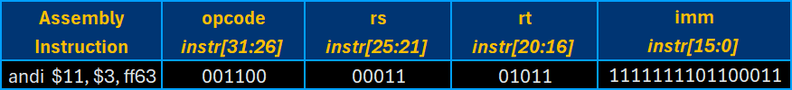
The I-type instructions also contain arithmetic operations and logical evaluations, like the R-type, but with different arguments and destinations. For argument values, I-type instructions use the value from the rs register address and the immediate (imm) defined within the instruction, saving the result to address given in rt.
This processor’s I-type instruction set includes the following operations, corresponding with their R-type equivalents and designated as immediate by the suffix ‘I’ added to their names:
- ADDI
- ANDI
- ORI
- XORI
Like the RISC-V instructions, not all R-type operations translate to I-type operations. The omitted equivalents to R-type instructions require additional logic beyond the scope of this processor design.

The I-type instructions also support Branch operations which use a different instruction interpretation than the previous example. Branch operations apply conditional logic to evaluate the values of rs and rt, and they change the program counter (PC) value by the imm value to calculate the target address, if the conditions are true.
This processor supports the following Branch operations:
- BEQ: Branch, if Equal (Branch executes when arguments are equal)
- BNE: Branch, if Not Equal (Branch executes when arguments are unequal.)
Branch instructions correspond to conditional logical used within programming languages that use cases to determine the flow of logic. Example cases include if/else conditions, loops, and switch statements.
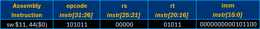
Unlike the RISC-V architecture, the MIPS I-type instructions contain both of the following “load” and “store” operations for 32-bit “word” values – instead of using dedicated S-type instruction set for “store” operations:
- LW: Load Word
- SW: Store Word
J-Type Instructions
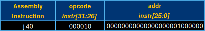
Jump instructions resemble the I-type Branch instructions but they use unconditional logic to determine the destination instead. This means Jump instructions always execute a move to another location within the program.
Pipelined Architecture

This processor uses the five pipeline stages, common to the reduced instruction set computer (RISC) ISA framework, but with additional resources and controls in place to prevent "hazards" arising from multiple instructions competing for simultaneous access to the same information and cases where subsequent instruction selections are pending. These additional resources include the Hazard Detection and Data Forwarding units that identify potential hazards – at various points within the pipeline – and mitigate them by stalling instructions or expediting the delivery of required resources. The pipeline registers between each stage support these modules by storing calculations from previous cycles required by the logic of these hazard mitigation units.
Hazard Types
Hazards, in relation to pipelined architecture, refer to conditions that prevent subsequent instructions from processing correctly due to conflicts with preceding instructions. These potential hazards fall within three categories: data, structural, and control hazards.
Data Hazards
Data hazards arise when an instruction depends upon a value from a preceding instruction that is not yet available, due to conflicting read and write operations. This processor design has the potential to create a specific type of data hazard known as a read after write (RAW) hazard. A RAW hazard arises when an instruction attempts to read a value from a register to which a preceding instruction has yet to perform a write operation.
Depending on specific conditions, the Data Forwarding and Hazard Detection units identify the potential hazard and mitigate it either by using either data forwarding or stalling, with the former being the preferred method.
Data forwarding involves the Data Forwarding unit accessing a value after its calculation, providing immediate access to the value before the following stage where the preceding instruction writes the value to the register.

In this example, the SUB instruction needs an argument value written by the ADD instruction in the following stage. The Data Forwarding unit accesses the necessary value after its calculation in the ADD instruction’s EX stage and delivers it to the SUB instruction. The label EX(F) denotes this Execution Forwarding behavior.
In cases like this, the Data Forwarding unit retrieves the required value from a Pipeline Register, designed as temporary storage locations to hold values from intermediary processor stages.
Another data hazard type exists beyond the mitigation capabilities of the Data Forwarding unit, known as “load-use” data hazards. These hazards involve values loaded from memory locations that are unavailable until the end of the MEM Stage.
The load-use data hazards require the use of stalling, or pausing the current instruction until the required resource becomes available at a later stage. Stalling requires the use of a “no operation (NOP)” instruction that prevents the instruction from accessing the necessary registers in the current cycle. An alternate description for using a NOP instruction is “inserting a bubble” because it represents an empty space within the pipeline.
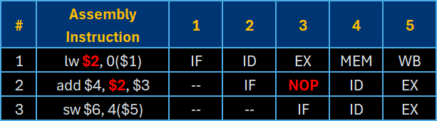
This example shows an ADD instruction that requires a value not available until the MEM stage of the preceding LW instruction. The processor implements the NOP in stage 3 to push the ADD instruction’s access to its ID stage in the following stage.
Control Hazards
Control hazards happen in response to branch and jump instructions, where the selection of the following instruction is pending. This minimal processor design mitigates control hazards through the simple methods of stalls and flushes, unlike classic MIPS implementations that include a branch delay slot. Stalls hold the subsequent instructions and flushes clear any pending, subsequent instructions, when a branch or jump instruction moves a new location outside of the current sequence.

In this example, the BEQ instruction’s conditional logic causes it to select the target instruction, making the two subsequent instructions – associated with not selecting the branch – irrelevant. The processor uses NOP to stall the pending instructions, choosing to load the target instruction instead. Then, in the following cycle, the processor flushes the skipped instructions.
Control hazards from branch instructions only occur upon branch selection (i.e., the fulfillment of branch conditions).
Structural Hazards
Structural hazards occur when multiple instructions require simultaneous access to the same processor component, in general. For example, a structural hazard results from simultaneous Data Memory access requested from both an LW and SW instruction, regardless of whether they target the same address or two distinct ones. The hazard occurs at the component level.
This processor design contains no explicit structural hazard mitigation controls, but the overall structure of the design provides inherent solutions to prevent these hazards. The design has separate memory modules for Instruction and Data Memory, accessible only from different stages, access to the ALU only occurs in the EX Stage, and the Register File is only accessible within the ID Stage and includes controls that prevent simultaneous read and write requests.
Technology
I used Lucidchart to design block diagrams to map stage-specific modules and interconnectivity throughout the entire design. I also used Vivado to develop design and testbench modules, and to export custom reporting used to debug and validate the design.
Development
This project includes distinct modules within each stage and general components – like multiplexers and pipeline registers – instantiated multiple times within different stages, in addition to the Data Hazard and Execution Forwarding units. The MIPS Processor module is the parent container for the entire design.
Development began with the design of unique components, followed by general, pipeline components. Next came the design of each stage, instantiating and connecting the respective components. Then, mapping signals to the intermediary pipeline registers between each stage. Finally, integration of the Data Hazard and Execution Forwarding modules, before encapsulating all stage, register, and control components into the MIPS Processor container.

The MIPS32 Processor is the parent container for the design, including the modules and buses that support the five-stage processing and hazard mitigation. The MIPS32 Processor module receives the clock and reset input signals, passing them to the necessary submodules, and returns the result output from each completed instruction, from the Write Back stage.
The following sections describe the modules for the pipeline stages and registers, followed by the hazard mitigation units.
Instruction Fetch (IF) Stage

The Instruction Fetch (IF) stage module centers around the Program Counter (PC) module that holds the address of the instruction to fetch, corresponding to those stored within the Instruction Memory module, and uses an adder to advance the instruction address to that of the following instruction.
The PC receives its next instruction address from a pair of 2:1 multiplexers that work together to select whether the PC receives the next instruction – iterated by the adder – or the address of a branch or jump instruction. The next instruction also depends on the stall control signal, from the Hazard Detection unit, which initiates an NOP instruction when needed. This lightweight design uses a 10-bit PC, which supports its minimal instruction set – as opposed to the full 32-bit implementation found in typical MIPS32 implementations.
The Instruction Memory module contains a series of instructions that initialize 10 register values, followed by a series of basic instructions and batches of instructions designed to trigger specific hazard mitigation responses. SW instructions follow each batch of tests, making the results available for evaluation.
/** InstrMem.v instructions for load-use RAW data hazard tests **/

/* RS Dependency Test */
rom[46] = 32'b10001100000010110000000000100100; // lw  $11, 36($0)
rom[47] = 32'b00000001011000100110000000100000; // add $12, $11, $2

/* RT Dependency Test */
rom[48] = 32'b10001100000011010000000000100000; // lw  $13, 32($0)
rom[49] = 32'b00000000001011010111000000100000; // add $14, $1, $13

/* Store Test Results */
rom[50] = 32'b10101100000011000000000001110100; // sw $12, 29($0)
rom[51] = 32'b10101100000011100000000001111000; // sw $14, 30($0)
This excerpt from Instruction Memory includes the instructions used to test and validate the processor’s response to “load-use” RAW data hazard cases. To simplify this article, all future analysis and commentary about specific instructions focuses only on this subset of instructions. The InstrMem.v file in the GitHub repository contains the entire instruction set, including a comprehensive amount of supporting information via comments.

This block diagram represents a group of pipeline registers between the Instruction Fetch and Instruction Decode (IF/ID) Stages. These temporary registers hold the value of the current instruction and the address of the following instruction.
The IF/ID Pipeline Registers have data hazard and flush control signals, from the Hazard Detection unit, to support stalling and flushing, as required. These control signals are unique to the pipeline registers at this phase, with only clock and reset controls appearing in subsequent instances.
Both output values from these pipeline registers pass through to the ID Stage, and the instruction output also passes to the Hazard Detection unit and the Instruction ID/EX Pipeline Registers, located beyond the next stage.
This Pipeline Registers block diagram – and all following Pipeline Registers diagrams – illustrates a simplified representation of these registers. The actual implementation involves a distinct register module for pair or input and output signals, instead of this consolidated version that contains all signal pairs. The enumeration of these signals corresponds to the distinct instances of these registers that appear within the MIPS32 Processor module.
Instruction Decode (ID) Stage

The ID Stage is the most complicated of all the stages within this design, handling register operations, the assignment of immediate values, calculations of values needed for branch and jump operations, and facilitating the control signals associated with the data and control hazard responses.
The register operations involve processing write, address, and data values from the Memory Access and Write Back registers to write result values to the register, as needed, the Register File module in the bottom/left of the diagram. This module also receives subsets of the instruction (instr) input from the IF/ID register to perform read operations, passing any required register values as output.
Other subsets of the input instruction value support the calculation of the immediate value, branch control signal, and addresses for the branch, jump, and destination register, with the aid of logical operators: shift registers, bit selectors, an adder, a comparator, and an AND gate, as illustrated in the bottom of the diagram. The top half of the diagram represents the output from the Controller module, which generates control signals for components in future stages, processed through a series of 2:1 multiplexers controlled by the hazard control code (Hazard_CC), calculated from the Hazard Detection unit output signals – denoted with red signals and components.
The Hazard_CC signal uses an OR gate to set it as active if it receives a data and/or control hazard signal from the Hazard Detection unit. The data hazard input is active low, requiring an invertor to trigger the following OR gate. In the event of a hazard, the Hazard_CC flushes all the connected 2:1 multiplexers by forcing them to output values of zero instead of the values received from the Controller module.
The Controller outputs for the branch and jump control codes bypass these hazard-controlled multiplexers, passing the jump control code directly to the module output and sending the branch control code into the selection logic flow previously mentioned.
The output signals pass to the next set of pipeline registers, except for those related to the branch and jump operations, which return to the IF Stage instead. These signals are the control codes at the bottom of the diagram (branch_sel and jump_sel) and the address values that appear in the lower/right (branch_addr and jump_addr).

The Instruction Decode / Execution (ID/EX) Pipeline Registers receive all the output values from the ID Stage and an instruction value from a preceding IF/ID Pipeline Register, as indicated at the bottom of the diagram.
An ID/EX Pipeline Register also receives the instruction value from the preceding IF/ID Pipeline Registers, as indicated at the bottom of the diagram.
Output signal destinations from the ID/EX Pipeline Registers scatter, with only five of them passing through the Execution (EX) Stage. The remaining signals, in addition to those split from the initial five signals, go to both hazard mitigation units and the EX/MEM Pipeline Registers.
Execution (EX) Stage

The Execution (EX) Stage generates two output values, based on an arithmetic logic unit (ALU) calculation and selections from a series of multiplexers and control signals. The ALU result output corresponds to a literal result from an arithmetic or logical operation, or the calculation of a memory address required for a load or store operation. The second output corresponds with a value for writing to a memory address in the following stage.
The ALU executes the operation specified by the control signal it receives from its ALU Controller module, after the latter calculates the operation by considering two input control codes from the previous stage. The data for ALU input “a” comes from the “Mux_Fwd_A” module and the other from the 2:1 multiplexer.
The 4:1 multiplexers receive control signals from the Data Forwarding unit to select from input values they both receive from a previous ALU result, stored in the following Pipeline Registers, and a result value from the Write Back (WB) stage – in addition to a distinct Reg value for each, read from the Register File in the previous stage.
The “Mux_Fwd_B” module output passes directly to the EX Stage output and to the 2:1 Multiplexer. Depending on the instruction type, determined by the ALU source (alu_src) control code, the 2:1 Multiplexer passes the previous input or the immediate value, received from the previous stage, to the ALU for its result calculation.

The Execution / Memory Access (EX/MEM) Pipeline Registers receive the two outputs from the previous stage, in addition to five signals it receives from the ID/EX Pipeline Registers.
The EX Stage outputs pass through these registers to the MEM Stage, along with the Mem Read and Mem Write control signals. The ALU result also passes back to the EX Stage and forward to the MEM/WB Pipeline Registers. The remaining output signals go to the Data Forwarding unit and MEM/WB Pipeline Registers.
Memory Access (MEM) Stage

The Memory Access (MEM) Stage consists of a single Data Memory module that performs memory read or write operations based on the combination of control signals and data values received from the EX/MEM Pipeline Registers. In the case of performing a read operation, it passes the value from the corresponding memory address to a MEM/WB Pipeline Register.

The Memory Access / Write Back (MEM/WB) Pipeline Registers contain values from the MEM Stage output along with four inputs from the EX/MEM Pipeline Registers.
The first two outputs are potential output values passed to the Write Back stage and the third is a control signal for the following stage. The last two output values contain register address and write control signal, passed to the ID Stage and to the Data Forwarding unit.
Write Back (WB) Stage

The Write Back (WB) Stage is a 2:1 Multiplexer, selecting either the value read from memory or previous ALU result.
The WB result passes through as the MIPS32 Processor result output and passes to the ID Stage for writing to a register and to the EX Stage as an input consideration for its ALU calculation.
Data Forwarding Unit

As previously mentioned, the Data Forwarding unit identifies and mitigates RAW data hazards by expediting the delivery of calculated values – or forwarding them – to instructions requiring these values before preceding instructions write them to a register.
The Data Forward unit manages this by collecting “write enable” signals, from both the EX/MEM and MEM/WB Pipeline Registers, instruction argument addresses from the ID/EX Pipeline Registers, and destination register addresses from the EX/MEM and MEM/WB Pipeline Registers.
Evaluating these input signals allows the Data Forwarding unit to verify the occurrence of a write operation, using the control signals, and to identify whether argument addresses from the ID/EX Pipeline Registers correspond with destination addresses from instructions further in the pipeline.
After this evaluation, the Data Forwarding module sends its forward A and B control signals – corresponding to the two instruction argument values rs and rt – to the 4:1 Multiplexers in the EX Stage to select the proper input signals: the Register File value from the ID/EX Pipeline Register, the ALU Result from the EX/MEM Pipeline Register, or the WB Result.
Hazard Detection Unit

The Hazard Detection unit mitigates load-use data hazards, beyond the scope of the Data Forwarding unit, and control hazards from branch and jump operations. The Hazard Detection unit identifies RAW data hazards with a load-use dependency by evaluating the “memory read’ control signal and destination address from the ID/EX Pipeline Registers and the argument values from the IF/ID Pipeline Registers to find a potential match between a LW register and an instruction argument. If this hazard exists, the Hazard Detection pushes the stall control signal to the IF and ID Stages and the IF/ID Pipeline Registers to insert a NOP instruction.
To mitigate control hazards, the Hazard Detection unit evaluates the branch and jump selection control signals. If it receives an active signal for either operation, the Hazard Detection unit pushes the flush control signal to the IF/ID Pipeline Registers and the ID Stage to clear any pending instructions from the pipeline.
Testing
The testing process ran concurrently with development – testing the functionality of components, stages, etc. through test benches and manual signal manipulation in the Vivado Simulation environment – and culminated with the development of the tb_MIPS32_Processor.v test bench, included within this project’s repository.
The final test bench includes 32 test cases to validate the execution of the following instructions from the processor’s Instruction Memory module.
- 10 initial register value assignments.
- 9 instructions to validate cases with no hazard mitigation.
- 9 instructions to validate the data forwarding responses for RAW data hazards.
- 2 instructions to validate the stalling responses for load-use RAW data hazards.
- 2 instructions to validate the stalling responses for control hazards.
This test bench returns results from these test cases via the following three methods, each providing a different level of specificity to provide high-level insights and pin-point analyses for resolving points-of-failure within the design.
- Scoring system and high-level performance summary.
- CSV file output with specific test details.
- Waveform diagram with specific details over time.
Simulation Time Constraints
This simulation exceeds the default Vivado limit and requires manual action to complete all tests and save the CSV file. Select “Run Simulation” to begin the tests, followed by “Run All” to complete the remaining tests.
Select “Run All” by one of the following:
- Click the ▶ icon on the upper toolbar.
- Select “Run” >> “Run All” from the top-level menu bar.
- Press the [F3] keyboard button.
Test Results
## Example Tcl score summary message

Test cases passed: XX / 22
After selecting “Run All,” this summary message appears in the Vivado Tool Command Language (Tcl) console, with ‘XX’ representing the number of valid test cases out of 22 (omitting the 10 initial register assignments). This output provides instant high-level performance feedback, confirming the correct execution of all tests or indicating the need to review the following, more detailed reporting.
/** Test bench snippet: Initializing and saving CSV output **/

integer f; // Output CSV variable

/** Initialize CSV file **/
initial begin
    f = $fopen("tb_mips32.csv", "w");
    $fwrite(f,"Test Condition,Expected,Actual,Result\n");
end

/** Close CSV file and finish simulation **/
initial begin
    #3000; // Delay until all test cases finish
    $fclose(f);

    $finish;
end
This snippet contains the Verilog assignments and blocks necessary to set up and finalize the comma-separated value (CSV) output file, named tb_mips32.csv. After defining the CSV variable, the first block opens the output file, in write mode, and prints the header row. The second block closes the CSV file prior to finishing the simulation.
The CSV output was my primary validation method because of the simple and targeted insights it offered, compared to the following waveform output.
## Example of CSV header and test case results

Test Condition,Expected,Actual,Result
...
Data Hazard (RS Dependency): ADD,d15f1416,00000000,FAIL
Data Hazard (RT Dependency): ADD,b54bc032,b54bc032,PASS
...
This example snippet from the CSV output file shows the heading values, followed by the rows of test feedback from the two “load-use” RAW data hazard cases.

After exporting the CSV data, I pasted into an Excel template that I created, using conditional formatting to emphasize specific points-of-failure. For example’s sake, I manually changed one of the actual result values to demonstrate an error response, but my final scorecard returned all accurate results and a score of 100%.
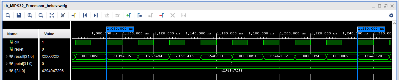
After identifying errors within the scorecard, I referred to the waveform output to identify points of failure and analyze adjacent results to discover root causes. This waveform snippet focuses on the same two cases as previous examples because the full waveform output is massive. The GitHub repository contains the entire waveform output, for reference.
/** Test bench excerpt: Load-Use RAW Data Hazard test cases **/

$fwrite(f, "Data Hazard (RS Dependency): ADD,d15f1416,%h,", uut.Data_Mem.ram[29]);
if(uut.Data_Mem.ram[29]==32'hd15f1416) begin
    $fwrite(f, "PASS\n");
    point = point + 1;
end
else $fwrite(f, "FAIL\n");

$fwrite(f, "Data Hazard (RT Dependency): ADD,b54bc032,%h,", uut.Data_Mem.ram[30]);
if(uut.Data_Mem.ram[30]==32'hb54bc032) begin
    $fwrite(f, "PASS\n");
    point = point + 1;
end
else $fwrite(f, "FAIL\n");
This snippet of code from the test bench shows the conditions for evaluating the two load-use RAW data hazard test cases. Each test case contains conditional logic to compare the expected and actual results from the corresponding memory address. The corresponding “PASS” or “FAIL” message prints to a row of the CSV file, including the actual value read from memory. A “PASS” result also includes an iteration of the point value.
/** Test bench excerpt: Results summary message **/

$display ("Test cases passed: %0d / 22\n", point);
Finally, the test bench executes a statement to display the Tcl performance summary message at the end of the test block, before finishing the simulation.
The insights from the three simulation outputs work together to create an effective troubleshooting workflow. The summary gives feedback on overall performance, the CSV output includes specific details about points of failure, and the waveform diagram provides context surrounding any points of failure and their impact on the entire system.
Credits
This project is a major update to a project I developed for the “Organization of Digital Computers Laboratory (EECS 112L)” course I completed at the Samueli School of Engineering at UC Irvine.
References
Project Results
The results generated by the final test bench confirmed the validity of the 22 test cases and the 10 initial register assignments. The implementation of multiple output methods allowed confirmation of success at a high-level by means of the score summary message and detailed analyses from the conditional feedback of the scorecard and manual inspection of the waveform output.
Despite MIPS32 being a legacy ISA, this project provided me with valuable experience for working with pipelined architecture and implementing controls to mitigate the potential hazards that come with it. I look forward to applying the fundamentals I learned from this project in the development of future projects using more modern and sophisticated ISA builds.
Takeaways
The overall complexity of this project required significant investment in planning, organization, and reporting to deliver a successful implementation of my processor design.
My investment in planning was the most significant factor in my success. Creating the schematics to design each processor component and mapping the buses between them provided me with an invaluable resource to ensure the proper interconnectivity and data flow for this design.
Adopting organized and consistent design practices allowed me to manage the complexity of this design and easily identify specific components and connections. For example, I used naming strict naming conventions for I/O signals and buses, with lowercase naming conventions for the former and Pascal case for the latter. I also added prepending stage and pipeline register labels, where applicable, to track the origins of the interconnecting bus signals.
Finally, implementing alternate reporting methods provided me with efficient alternatives to a sole reliance upon the massive and complex waveform diagram – the default Vivado output method. The score summary provided me with instant feedback on the overall system performance and the global impact of changes I made. My custom dashboard expedited my ability to pinpoint specific failures and uncover root causes over performing the same analyses by reviewing the waveform diagram.
Next Steps
Since MIPS32 is a legacy ISA, I have no plans to optimize this design or invest in expanding its instruction sets and capabilities.
However, I do plan to implement this processor design – or a derivate of it – to program a field-programmable gate array (FPGA) and test the design’s ability to drive a hardware project.
Feedback
Thank you for reviewing my project. I hope you found it insightful. Please contact me if you have any questions or feedback about this specific project – or my work in general.
Recent Projects
If you enjoyed this project, please consider reviewing one of my recent projects below.